|
Laser Diode Pump Assembly
Laser Diode assemblies manufactured by Spectra Devices Laboratory (SDL) were procured for the GLAS instrument on the ICESAT spacecraft and for the Calypso Program as pumps for the YAG bars in the laser systems. The semiconductor devices consist of an AlGaAs active region epitaxially grown on a GaAs substrate. The 1.00 cm long, rectangular semiconductor die, or “Diode Bar” contains many emitters, 79 in GLAS’s device (whose die height is 730 µm). It is attached with eutectic SnPb solder to a gold-plated, Copper-Tungston submount (CuW – 10%/90%) (Fig.1). An alumina spacer, coated on top and bottom with a gold film, is also soldered with SnPb eutectic solder to the sub-mount parallel to the diode bar (Fig. 2). One mil gold wires are wedge-bonded between the laser bar and the alumina spacer bar (Fig. 3). In the GLAS device, 1 mil wire was used to create six groups of fifteen wire bonds down the length of the diode bar. The wire bonds were made with lengths that alternated between, 0.55mm, 0.75 mm and 0.95 mm (short, medium, long from right to left down the diode bar).
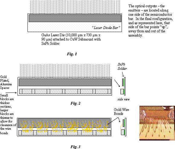
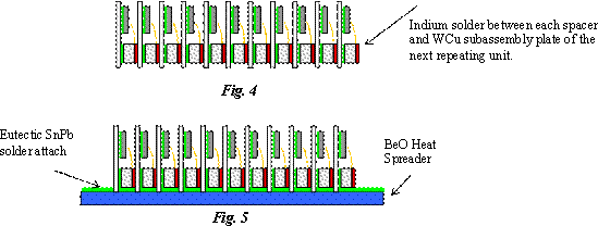
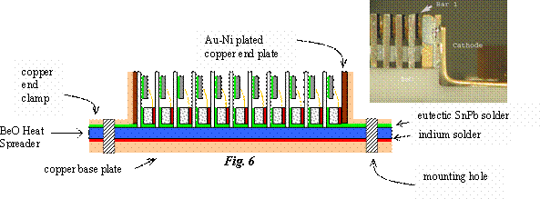
To achieve the necessary optical output power of the final subassembly, multiple copies of this subassembly of CuW sub-mount with attached laser diode bar and ceramic spacer (connected using wire bonds), are stacked and soldered together into a continuous, many-deckered sandwich using 99.9% pure Indium solder between the raised bosses on the alumina spacers of one unit, and the backside of the CuW sub-mount of the next unit. Each end is soldered to a thick copper end-block (Fig. 4). The number of repeating units depends on the user’s power output needs and is identified in the generic part number. The G9 has nine repeating units; the G16 has 16 and so on. Calypso used the G16’s; MOLA the G9 and GLAS used G2, G4 and G11 types. The G11 part used by GLAS operates with a pulsed, (200 µs pulses at 40 Hz) 100 A current. The entire array or final “sandwich” is attached with eutectic SnPb solder to a BeO slab which provides mechanical support and a heat sink to the sandwich while maintaining the series electrical connection through the wire bonds (Fig. 5). The BeO slab is then attached to a copper plate, with 10 µm thick indium solder, that provides heat sinking to the chassis. Copper end-clamps are used to keep the sandwich in place and to provide the anode and cathode connection (Fig. 6). The gold plating, the wire bonds, the conductive W-Cu material and the Indium solder provide a continuous electrical path from one end of the sandwich to the other end. The resulting electrical configuration is a series connection of the laser bars between the anode and the cathode. The thermal circuit allows each of the diode bars to thermally conduct to the BeO heat spreader in parallel. The mounting holes are drilled through both the copper plate and the BeO heat spreader at each end of the assembly.
The type of laser assembly used by GLAS was examined as part of a failure investigation following an in-flight failure. The assembly was studied and disassembled and significant amounts of indium-gold intermetallic material were found all around and on the gold wire bonds (Fig. 7). Some of the intermetallic material, much greater in volume (nearly four times larger)139 than the original gold wire, was massive enough to bridge the space between adjacent subassemblies causing them to be broken when the sandwich was disassembled. The intermetallic, consisting of several phases, is much more brittle than the original gold material.139
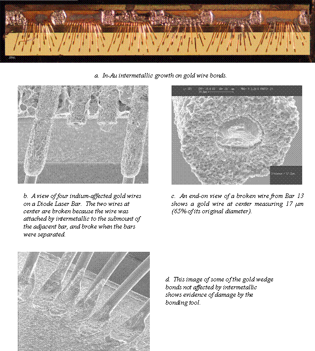
Indium-gold intermetallic growth on gold wire bonds (Fig. 7).
Several methods were used in the FA (failure analysis) of the G11 unit used by GLAS: Focused Ion Beam (FIB) crossectioning, Scanning Electronic Microscopy (SEM), Energy-Dispersive Spectroscopy. Longitudinal FIB cuts into the wires and examination of broken wires showed that the gold material was not fully consumed by the intermetallic though the diameter of the gold was reduced by as much as 30%. The data also showed that on the leading edge of the intermetallic growth, the gold content within the intermetallic region was higher at the outer edge of the material and where it was nearest the host gold, while the material was indium-rich near the center of the intermetallic. At the trailing edge, the intermetallic was more elementally homogeneous.
Other observations of the same sample showed highly flattened wedge bonds that appeared to be caused by the use of a bonding tool that was too big for the clearance available. There was also a lack of a good metallic bond between the sandwich assembly and the BeO heat spreader. It is possible that the lack of a sufficient thermal conduction path from the laser diode bars through the heat spreader caused a severe thermal gradient between the center of the assembly to each end where the only other serviceable thermal path existed. This large thermal gradient could have created a thermal cycling condition at turn-on and turn-off causing the fragile dissolved gold wire to fracture. As the wires broke, the increased current in the remaining wires would exacerbate the thermal stress causing more wires to break. The last wires to remain would be vaporized due to the very high current they would be carrying. Failure of an entire bar would break the series electrical connection. The FA’s performed at NASA GSFC resulted in several reports including:
Laser Diode Array, Spectra Devices Lab, Goddard Space Flight Center Report, Report Number Q30219FA B670, Frederick Felt, QSS, August 2003
Laser Diode Destructive Physical Analysis Report for CALIPSO, Goddard Space Flight Center Report, Report Number Q30275EV, Frederick Felt, QSS, September 2003 (pending approval).
A NASA Alert was also published about the danger of co-locating indium with gold bond wires. This alert contains photographs and experimental results that illustrate the rapid-growth of Au-In intermetallic species at room and ground testing temperatures. A link to this alert is:
NASA Advisory NA-GSFC-2004-01, Indium Solder Encapsulating Gold Bonding Wire Leads to Fragile Gold-Indium Compounds and an Unreliable Condition that Results in Wire Interconnection Rupture, H. Leidecker, 9/23/03
Jane Jellison performed some focused experiments on Au-In compound formation for the TIROS project in 1979. Her findings, edited by Dr. Henning Leidecker are in this paper: Gold-Indium Intermetallic Compounds: Properties and Growth Rates, Jane E. Jellison, NASA GSFC Code 313, Materials Control and Applications Branch (MC&AB), 11/8/79 , Ed. H. Leidecker, 7/03.
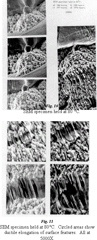
She found that Au-In intermetallics grow readily at high temperature (140°C ad 120°C) and relatively quickly at temperatures as low as 40°C (Fig. 8, 9). The indium was found to be highly mobile, moving well beyond the original Au-In interface. The high mobility of the indium atoms creates voids in the area where the gold (now Au-In intermetallic) was in direct contact with the indium coating. The large grained, columnular structure of the intermetallic was also found to be strong enough to create plastic deformation in the indium at the interface and to force the gold out of contact with the indium (Fig. 10, 11). In test samples where gold bonds had been overcome by indium and intermetallics were created, bond pull strengths were found to have decreased by over 40%. The resistivity of the intermetallic material was found to be about four times that of gold.
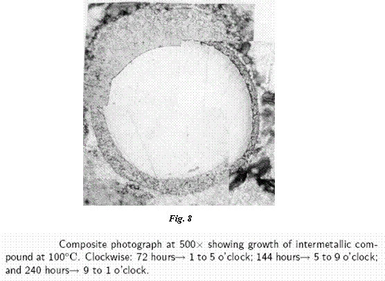
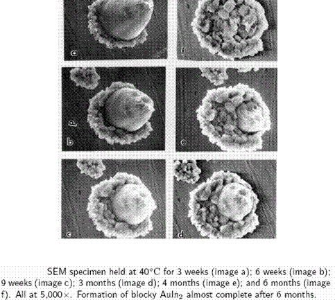
Fig. 9
Jellison found that AuIn and AuIn2 compounds created in the laboratory for experimentation were very brittle showing no evidence of plastic deformation at the fracture sites. She references similar work that was done on intermetallics formed at a Pb-In and Au interface. Similar growth rates and AnIn species were found in the experiments with Pb-In and Au as was found with In and Au and no Pb. The difference was that the Pb was left at the interface, which actually contributed to the system’s mechanical strength.
Using the growth rates calculated from the data accumulated through a matrix of time/temperature experiments on gold wire embedded in indium, Jellison calculates the temperature required to limit intermetallic growth to 1 µm over 4 years. She accounts for growth that will occur during processing and storage. Assuming an unlimited supply of indium, the calculations showed that a 12.8 µm layer would be present after four years with a storage temperature of 20°C (An actual flight detector had been found to have an In-Au intermetallic layer of 10 µm after four years of storage). To achieve the 1 µm goal, the storage temperature would have to be 0°C or less.
Jane Jellison’s conclusions are worth repeating here:
- The growth rate of AuIn2 is not negligible at room temperature.
- Current processing techniques are very likely to form significant amounts of AuIn2.
- The reaction product AuIn2 occupies more space than did the reactants and its presence can lead to fracture or separation of the bonded area.
- The reaction product is a good electrical conductor, and, provided mechanical integrity in the bond area is maintained, its presence would not affect the operation of the device.
- The mechanical properties of the reaction layer are very poor; it tends to form loosely bonded blocky crystals and is extremely friable.
- From conclusions 4 and 5, there is no non-destructive way of determining whether a properly functioning device has very weak bonds.
- Long term storage of detectors with gold and indium in the bond area should be at low temperature – the exact temperature being determined by what is considered an acceptable growth rate (Going from 20°C to 0°C retards the growth rate by about a factor of 3).
|