|
|
|
|
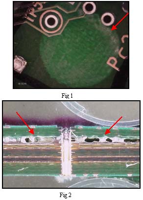
Delamination of PWB in Vapor Phase Soldering |
|
2. PWBs: Delamination of PWB during vapor phase soldering
The delamination above occurred during the Vapor phase re-flow assembly process. The delamination was the result of problems with the manufacture of the PWB and or not baking out the board prior to soldering. The NASA standard requires the bake-out of PWB prior to exposing the board to soldering temperatures.
Reference :
NASA-STD-8739.3
Delamination. A separation between plies within a base material or any planar separation within a multilayer PWB.
7.3 Preparation of Printed Wiring Boards, Terminals, and Solder Cups
3. The PWB's shall be cleaned and demoisturized within 8 hours prior to their initial exposure to soldering temperatures. The PWB's may be stored for longer periods of time in a controlled moisture-free atmosphere. Demoisturizing may be accomplished by an oven bake at 93°C (200°F) ±5.5°C (±10°F) for a minimum of 4 hours for a printed wiring assembly (PWA) or 2 hours for a bare PWB, or by a vacuum bake at a lower temperature. The time in and out of the oven or chamber shall be recorded.
|
|
|