NASA - Home NEPP Home PagePartsPackagingRadiationAbout NASA Electronic Parts and Packaging (NEPP) Program
 
 Location:   Home  |  Workmanship Standards  |  Workmanship Problems Pictorial Reference  |  Printed Wiring Board Problems  |  Delaminated Trace

Also on this page:

 
Delaminated Trace

4. PWBs:  PWB trace damage

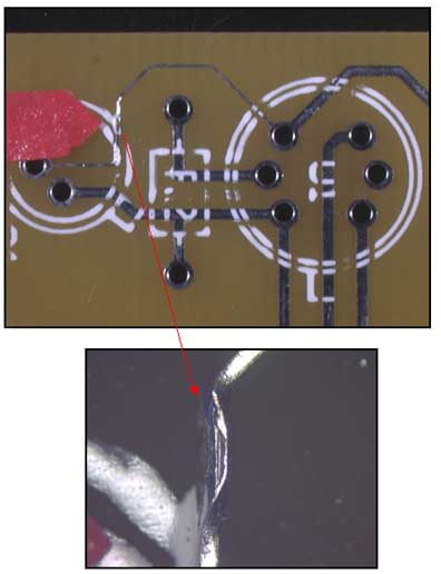
This board showed trace damage on receipt. The board apparently received a blow of some kind that tore the trace away from the board surface. The damage occurred after silk screening as evidence of the silkscreen being separated from the board.

Reference :
NASA-STD-8739.3
5. Pattern Repair.
Repair of damaged or broken conductor patterns on PWB's is not permitted.
d. Verify that no damage exists on parts or PWB's prior to being assembled and soldered. In addition, parts and PWB's shall be inspected to verify that solderability has been maintained.


Close up of delaminated pwb trace