|
|
|
|
Wave Solder Process Problem |
|
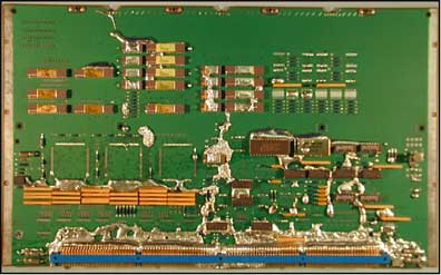
15. PWAs: Wavesolder process problem
This is a board, which has gone thru wave solder. There was a process problem either incorrect wave height and or board sagged due to not being properly supported in fixture going over wave. Resulting in scrap board.
Reference :
NASA-STD-8739.3 par. 12.1
General
This chapter contains requirements peculiar to automatic wave soldering.
1.The supplier's process documentation for automatic wave soldering operations shall define: a.Preheat temperature b.Temperature of the solder. c.Conveyor speed and angle. d. Height of the solder wave e. Flux density. f. Flux height. g. Depth of PWA in wave h. Control of the dross inhibitors i.Allowable contaminants when the solder bath is analyzed j. Frequency of maintenance and of analysis and other factors affecting the quality of the connections in the end product.
12.4 Wave Soldering
1.The preheat temperature shall be maintained within 2 °C (5 °F).
2.The conveyor speed shall be controlled to a preselected rate and shall not vary more
than 2.54 cm (1 in.) per minute.
3.Solder temperature shall be controlled so that the solder in the wave is 250 °C (482 °F)
to 275 °C (527 °F).
4.The height of the solder wave shall be controlled to a constant preselected height.
|
|
|