|
|
     |
 |
|
Location:
Home |
Workmanship Standards |
Workmanship Problems Pictorial Reference |
Parts and Components |
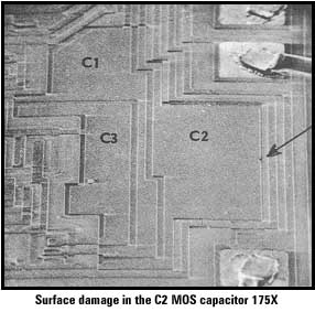
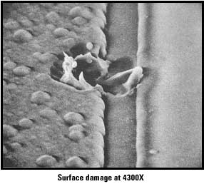
Microcircuit ESD Damage
|
|||
|
|
||||||||
|
|
NASA Officials: Peter Majewicz, Program Manager Jonathan Pellish, Deputy Manager Webmaster: Carl M. Szabo, Jr. Last Updated: Dec 2, 2008 3:26PM |
>Contact NEPP |
>NASA Privacy Policy and Important Notes |