|
|
|
|
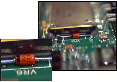
Conformal Coating Under Diode |
|
4. Components: Conformal Coating Under Diode
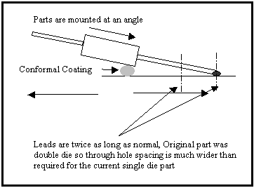
This diode was mounted with leads twice as long as would normally be required along with slight tilting of the part body. The result was a build up of excessive conformal coating accumulating under one end of the part body, which resulted in a stress to the solder joints and component.
Reference :
NASA-STD-8739.1
2. Acceptance Criteria. Conformally coated PWA's shall exhibit, as a minimum, the following workmanship characteristics to be acceptable: f. Conformal coating shall be uniform in thickness as specified in Table 10-1 or on engineering documentation except in touched-up areas as per paragraph 10.5.
APPENDIX A CONFORMAL COATING PROBLEMS
The following are the major problems encountered in the conformal coating process:
1. Conformal Coating Thickness. Conformal coating thickness can be critical to the proper function of a PWA. If a coating is too thin, proper coverage is impossible; if a coating is too thick, it may create excessive stresses on solder joints and components (particularly glass-bodied components). Controlling coating thickness is of special importance with rigid coating materials (e.g., epoxies and some of the urethanes) because the residual stresses associated with an excessively thick application of these materials are much greater than with flexible coating materials (such as silicones and some urethanes).
|
|
|